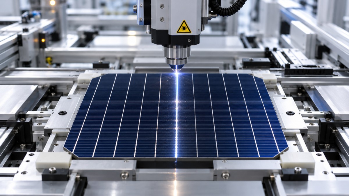
How does laser cutting affect solar cell efficiency?
auth.Dr. Liang ChenTime
Oct 30, 2026Click Count
Laser cutting affects solar cell efficiency in two competing ways. It can enable half-cell module designs that reduce resistive losses, yet the cut itself can introduce edge defects that increase carrier recombination and reduce the electrical performance of each cell piece. A module may therefore produce more power even when its cut cells perform slightly worse than the original full cells.
For technical evaluators, the important question is not whether laser cutting is inherently beneficial or harmful. It is whether the electrical gains from the chosen cell and module design outweigh cutting-related losses—and whether those gains remain credible after manufacturing variation and reliability testing are considered.
Why solar cells are cut in the first place
In crystalline silicon photovoltaic manufacturing, laser cutting is commonly used to divide a finished or nearly finished solar cell into smaller pieces. Half-cell modules are the best-known example, although smaller cell formats are also used in some designs. The cut cells are then interconnected according to the module’s electrical architecture.
The attraction is straightforward: a smaller cell has less active area and therefore generates less current under the same illumination. A half cell produces approximately half the current of the original full cell, while its voltage remains broadly comparable, assuming similar material quality and operating conditions.
That current reduction matters because resistive power loss follows the relationship P = I2R. Lower current can reduce losses in cell metallization and interconnections. Module designers can use those savings to improve power output, provided that the interconnection scheme and the added manufacturing steps do not erase the benefit.
However, “half the current” does not mean every resistive loss in the completed module falls to one quarter. A half-cell module has a different circuit arrangement, additional cell pieces and interconnections, and resistance distributed throughout the device. A meaningful comparison must account for the whole module, not just one conductor.

The trade-off: lower current, more exposed edge
Cutting creates new cell edges. Those edges are not simply geometric boundaries; they are regions where the semiconductor and its surface treatments may have been disturbed. Defects at or near the cut can act as recombination sites, where charge carriers disappear before they contribute to useful current.
For an evaluator reviewing a production process, the risk is easy to underestimate. A cut may look clean to the naked eye while still leaving electrically active damage. Conversely, a visually irregular edge is a reason to investigate, but it does not by itself establish the size of the electrical loss.
Recombination and voltage loss
Laser energy can disrupt silicon, dielectric passivation layers and other structures close to the cut. Depending on the process, it can also leave debris, microcracks or regions affected by heat. These changes may increase recombination and reduce open-circuit voltage, fill factor or both. The magnitude depends on the width and severity of the affected region, as well as the original cell’s properties.
Cutting also changes the ratio of edge length to active area. As cells are divided into smaller pieces, newly created edges represent a greater share of the device geometry. That makes edge quality increasingly important when comparing half cells with more aggressively segmented designs.
Shunts, cracks and mechanical handling
In some circumstances, cutting-related damage or conductive material near an edge can create leakage paths, contributing to shunting and a lower fill factor. Microcracks are another concern: they can interrupt current collection or become more significant during subsequent handling, interconnection and service stresses.
Not every crack or dark region has the same consequence. Its location, extent and effect on current paths matter. Electrical measurements should therefore be interpreted alongside imaging and mechanical observations rather than replaced by them.
How much efficiency can be gained—or lost?
There is no universal efficiency adjustment for laser cutting. The result depends on the starting cell, the cut process, the size and number of pieces, and the module design. Comparisons become particularly misleading when cell efficiency and module efficiency are treated as interchangeable.
For example, comparing a full cell’s absolute short-circuit current with that of a half cell is not a direct measure of cutting damage: the half cell has approximately half the area. Normalized current density and properly defined efficiency are more useful. Even then, measurements must account for differences in contact method, illumination and the area included in the calculation.
At module level, a power increase should not automatically be credited to the cutting process alone. Changes in metallization, interconnection, packing density or cell technology may contribute. Ask whether the comparison isolates the cell format or combines several design changes.
Which laser cutting parameters matter most?
Manufacturers use different approaches, including laser scribing followed by mechanical separation and laser-assisted separation processes. Some use thermal stress to guide a crack; others remove more material along the cutting path. The relevant settings are process-specific, so a parameter that works for one tool or cell stack should not be assumed suitable for another.
- Laser wavelength and pulse characteristics: These affect how energy is absorbed and how it interacts with silicon, coatings and metallization.
- Energy input and cutting speed: Insufficient or excessive energy can produce different defects. The objective is a controlled separation with minimal electrical and mechanical damage, not simply the fastest cut.
- Focus, alignment and cut location: Variation can alter the affected region or bring the process too close to sensitive features.
- Separation and handling: The mechanical step after scribing, along with transport and interconnection, can introduce cracks even when the initial laser process is well controlled.
- Edge treatment and cleaning: Where used, post-cut treatments may reduce damage, contamination or recombination. Their effectiveness should be demonstrated electrically and assessed for compatibility with later module processing.
A useful process window balances throughput against performance and yield. Evaluators should look beyond a single optimized sample and ask how consistently that window is maintained across production batches, cell suppliers and tool maintenance cycles.
Does the cell technology change the answer?
Yes. PERC, TOPCon, heterojunction and other cell architectures differ in their surface passivation, contact structures and sensitivity to thermal or mechanical disturbance. The same cutting recipe can therefore produce different results on different cells.
For example, an N-type TOPCon cell’s performance depends in part on the integrity of its passivating contact structures. A cutting process that damages the edge or nearby layers may undermine some of the benefit of a high-performing starting cell. Heterojunction cells also use layer stacks that require careful thermal and process compatibility assessment. These are reasons for technology-specific validation, not grounds for assuming that one architecture is always more vulnerable than another.
When reviewing a supplier’s evidence, check that the tested cell technology, wafer format and metallization match the proposed production configuration. Data from an earlier cell generation may be informative, but it is not a substitute for qualification of the actual design.
What should a technical evaluation include?
A strong assessment connects before-and-after cell measurements with finished-module performance. It also distinguishes cutting damage from losses introduced during handling, interconnection and lamination. That distinction matters when a module’s measured power falls short: without traceability, a supplier may struggle to identify which process step is responsible.
1. Establish a defensible electrical baseline
Request measurements of representative cells before cutting and of the resulting pieces after cutting, with the measurement method and area definitions clearly stated. Review open-circuit voltage, short-circuit current or current density, maximum power and fill factor. Where available, compare distributions across a meaningful sample rather than relying on one average value.
Look for paired or otherwise well-matched comparisons. Differences in illumination, temperature, contacting and calibration can obscure a small process loss. Measurements after additional processing should be identified separately so that any recovery or further damage is not incorrectly attributed to the cut itself.
2. Connect electrical results to physical evidence
Electroluminescence imaging can help reveal cracks, inactive areas and some nonuniformities. Microscopy can support examination of cut-edge morphology, debris and damaged layers. Depending on the investigation, photoluminescence, thermal imaging or other diagnostic methods may add useful information.
These tools answer different questions. A supplier should be able to explain how an observed feature relates to electrical performance and whether it changes after module assembly or stress testing. A collection of images without measurement context is less persuasive than a documented correlation.
3. Review the completed module and its reliability
Check module power measurements, cell-to-module loss analysis and the circuit layout. Then examine how performance changes after relevant environmental and mechanical stresses. Thermal cycling, humidity exposure and mechanical loading can reveal weaknesses that are not obvious immediately after production, although a test result alone may not identify the exact failure mechanism.
Ask for traceability between the tested samples and the commercial bill of materials. A qualified module design may not represent a later change in cell source, cutting equipment or interconnection method unless the manufacturer has assessed that change.
Relevant standards—and their limits
IEC 61215 addresses design qualification and type approval for terrestrial photovoltaic modules, while IEC 61730 covers module safety qualification. For electrical characterization, IEC 60904-1 describes measurement of photovoltaic current-voltage characteristics, and IEC 60904-3 addresses measurement principles including reference spectral irradiance. The applicable editions, test conditions and laboratory procedures should be confirmed for the project.
These standards provide a useful framework for consistent module and measurement evaluation, but they do not prescribe a universal acceptable laser-cut edge or prove that a particular cutting recipe is optimal. A passing module qualification result should be considered alongside process controls, production data and change-management evidence. Where certification is claimed, verify its scope and applicability to the proposed product rather than assuming it covers every manufacturing variation.
Questions worth asking before selecting a module
- What cell architecture, cutting method and number of pieces are used in the proposed module?
- How are cutting-related electrical losses measured, and are results reported as distributions as well as averages?
- Which inspections detect edge damage, cracks and shunting, and what are the acceptance criteria?
- Does the module-level power comparison isolate cell format from other design changes?
- What reliability evidence exists for the actual cell, interconnection and module configuration?
- How are equipment adjustments, cell-supplier changes and process deviations controlled?
The practical conclusion is nuanced: laser cutting can support higher module output by enabling lower-current cell layouts, but it also creates an edge that must be managed. The best evidence is not a claim that cutting improves efficiency; it is a traceable set of cell measurements, module results and reliability data showing that the complete design delivers its expected performance consistently.
Next:Already The FirstGot questions about this topic or seeking best practices for your project? Drop us a line below, and let Hengda Engineering's experts help you out.
Recommended News
- 00
0000-00
How does laser cutting affect solar cell efficiency?Discover how laser cutting affects solar cell efficiency, from lower resistive losses to edge damage, and learn how to evaluate module performance. - 00
0000-00
Thai Cabinet Approves THB 50 Billion Rooftop Solar Subsidy PlanThailand’s THB 50 billion rooftop solar subsidy plan targets one million homes and 5 GW. Explore household support, 20-year power resale and potential opportunities for solar suppliers. - 00
0000-00
How Do You Compare Solar Module Failure Rates Across Field Studies?How do I compare solar module failure rates from different field studies? Discover how to align definitions, exposure, and uncertainty to make smarter procurement and asset management decisions.
000000-00
{item.title}{item.description}Search News
Industry Portal
Hot Articles
- How does laser cutting affect solar cell efficiency?Discover how laser cutting affects solar cell efficiency, from lower resistive losses to edge damage, and learn how to evaluate module performance.
- BNEF Raises US Energy Storage Forecast 30% as Data Center Orders MaterializeUS energy storage forecasts rise 30% as data center orders materialize. Explore BNEF's deployment outlook through 2036 and what it means for the market.
- How custom metal fabrication protects DC chargers from rainDiscover how custom metal fabrication protects DC chargers from rain with engineered seals, smart drainage, and cooling design. Learn what to check for lasting outdoor reliability.
Popular Tags